- 您现在的位置:买卖IC网 > Sheet目录362799 > EVAL-AD1935EB (Analog Devices, Inc.) 4 ADC/8 DAC with PLL, 192 kHz, 24 Bit CODEC
Preliminary Technical Data
AD1935/AD1936/AD1937/AD1938/AD1939
Pin No.
36
37
38
39
40
41
42
43
44
45
46
47
48
49
50
51
52
53
54
55
56
57
58
59
60
61
62
63
64
Rev. Pr
I
| Page 19 of 30
In/Out
O
O
O
O
O
O
O
O
I
I
I
O
I
I
O
I
I
I
I
I
I
I
I
O
I
Mnemonic
OL1
OR1
OL2
OR2
AGND
AVDD
AGND
FILTR
AGND
AVDD
CM
ADC1LP
ADC1LN
ADC1RP
ADC1RN
ADC2LP
ADC2LN
ADC2RP
ADC2RN
LF
AVDD
Description
DAC 1 Left Output.
No Connect.
DAC 1 Right Output.
No Connect.
DAC 2 Left Output.
No Connect.
DAC 2 Right Output.
No Connect.
Analog Ground.
Analog Power Supply. Connect to analog 3.3 V supply.
Analog Ground.
Voltage Reference Filter Capacitor Connection. Bypass with 10 μF||100 nF to AGND.
Analog Ground.
No Connect.
No Connect.
Analog Power Supply. Connect to analog 3.3 V supply.
Common Mode Reference Filter Capacitor Connection. Bypass with 10 μF||100 nF to AGND.
ADC1 Left Positive Input.
ADC1 Left Negative Input.
ADC1 Right Positive Input.
ADC1 Right Negative Input.
ADC2 Left Positive Input.
ADC2 Left Negative Input.
ADC2 Right Positive Input.
ADC2 Right Negative Input.
PLL Loop Filter, Return to AVDD.
Analog Power Supply. Connect to analog 3.3 V supply.
No Connect.
No Connect.
Table 15. Pin Function Description—64-Lead LQFP (AD1935)
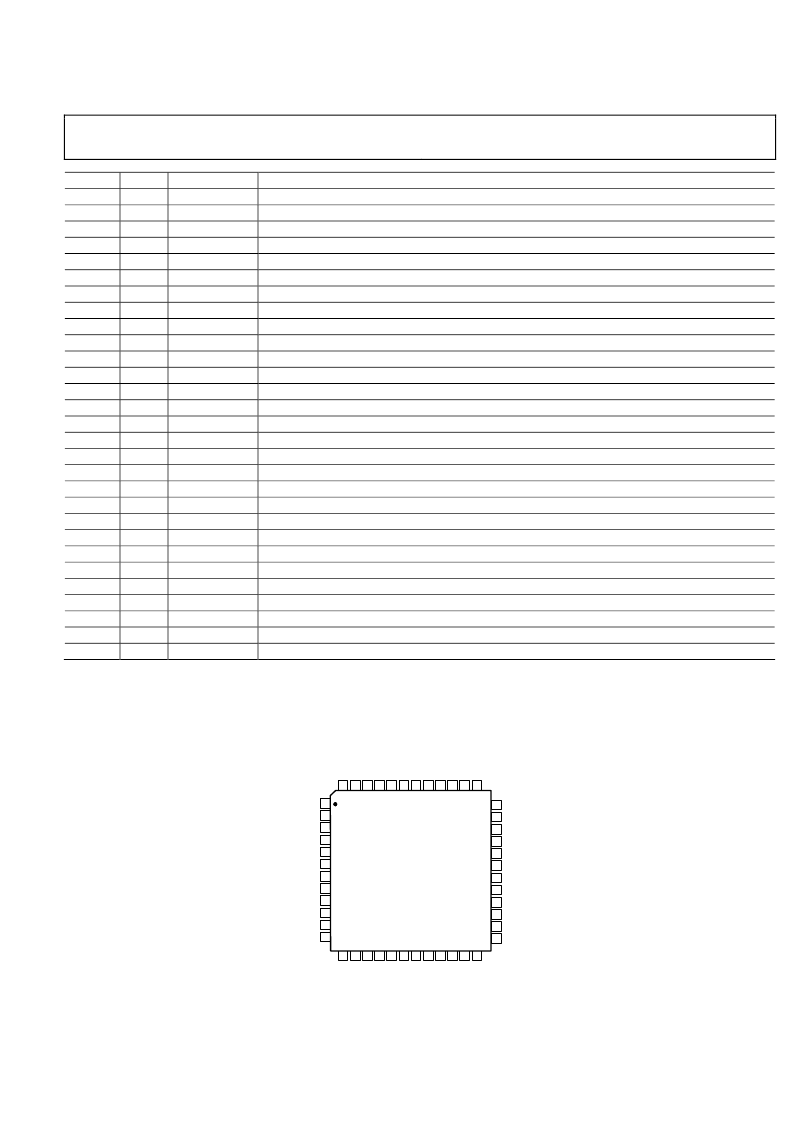
PIN CONFIGURATION
36
35
34
33
32
31
30
29
28
27
26
25
13 14 15
16 17 18 19 20
21 22 23 24
1
2
3
4
5
6
7
8
9
10
11
12
48
47 46
45 44
39 38
37
43 42
41 40
TOP VIEW
(Not to Scale)
Single-ended
Output
AGND
AVDD
AGND
OR2
OL2
OR1
OL1
CLATCH
/ADR1
CCLK/SCL
DGND
L
AGND
AVDD
OL3
OR3
OL4
OR4
PD/RST
DSDATA4
DGND
D
D
D
A
AGND
MCLKI/XI
MCLKO/XO
AD193X
A
A
A
A
A
A
A
A
C
FILTR
AGND
A
D
D
D
A
A
A
A
C
C
Figure 20. Single-ended Output 48-Lead LQFP (AD1936, AD1938)
Preliminary
发布紧急采购,3分钟左右您将得到回复。
相关PDF资料
EVAL-AD1936EB
4 ADC/8 DAC with PLL, 192 kHz, 24 Bit CODEC
EVAL-AD1937EB
4 ADC/8 DAC with PLL, 192 kHz, 24 Bit CODEC
Eval-AD1940EB
SigmaDSP-TM Multichannel 28-Bit Audio Processor
EVAL-AD1953EB
16-bit fixed point DSP with Flash
EVAL-AD1958EB
PLL/Multibit DAC
EVAL-AD1959EB
PLL/Multibit DAC
EVAL-AD1974EB
4 ADC with PLL, 192 kHz, 24-Bit Codec
EVAl-AD1974EBZ
4 ADC with PLL, 192 kHz, 24-Bit Codec
相关代理商/技术参数
EVAL-AD1936EB
制造商:AD 制造商全称:Analog Devices 功能描述:4 ADC/8 DAC with PLL, 192 kHz, 24 Bit CODEC
EVAL-AD1937AZ
功能描述:BOARD EVAL FOR AD1937 RoHS:是 类别:编程器,开发系统 >> 评估演示板和套件 系列:- 标准包装:1 系列:PSoC® 主要目的:电源管理,热管理 嵌入式:- 已用 IC / 零件:- 主要属性:- 次要属性:- 已供物品:板,CD,电源
EVAL-AD1937EB
制造商:AD 制造商全称:Analog Devices 功能描述:4 ADC/8 DAC with PLL, 192 kHz, 24 Bit CODEC
EVAL-AD1937EBZ
制造商:Analog Devices 功能描述:EB SINGLE CHIP CODEC 4 ADC'S W/DIFF OUTP - Boxed Product (Development Kits)
EVAL-AD1938AZ
功能描述:BOARD EVAL FOR AD1938 RoHS:是 类别:编程器,开发系统 >> 评估演示板和套件 系列:- 标准包装:1 系列:PSoC® 主要目的:电源管理,热管理 嵌入式:- 已用 IC / 零件:- 主要属性:- 次要属性:- 已供物品:板,CD,电源
EVAL-AD1938EB
制造商:AD 制造商全称:Analog Devices 功能描述:4 ADC/8 DAC with PLL, 192 kHz, 24-Bit CODEC
EVAL-AD1938EBZ
制造商:Analog Devices 功能描述:EVAL BD FOR MULTI CHANNEL 96KHZ CODEC - Boxed Product (Development Kits)
EVAL-AD1939AZ
功能描述:BOARD EVAL FOR AD1939 RoHS:是 类别:编程器,开发系统 >> 评估演示板和套件 系列:- 标准包装:1 系列:PCI Express® (PCIe) 主要目的:接口,收发器,PCI Express 嵌入式:- 已用 IC / 零件:DS80PCI800 主要属性:- 次要属性:- 已供物品:板